
IBM's 0.7nm Nanostack: What the First Sub-Nanometer Chip Means for Local AI
IBM just unveiled the world's first 0.7 nanometer chip technology, packing nearly 100 billion transistors onto a fingernail-sized die. Here is what the paper says, and why it matters for AI that runs on your machine.

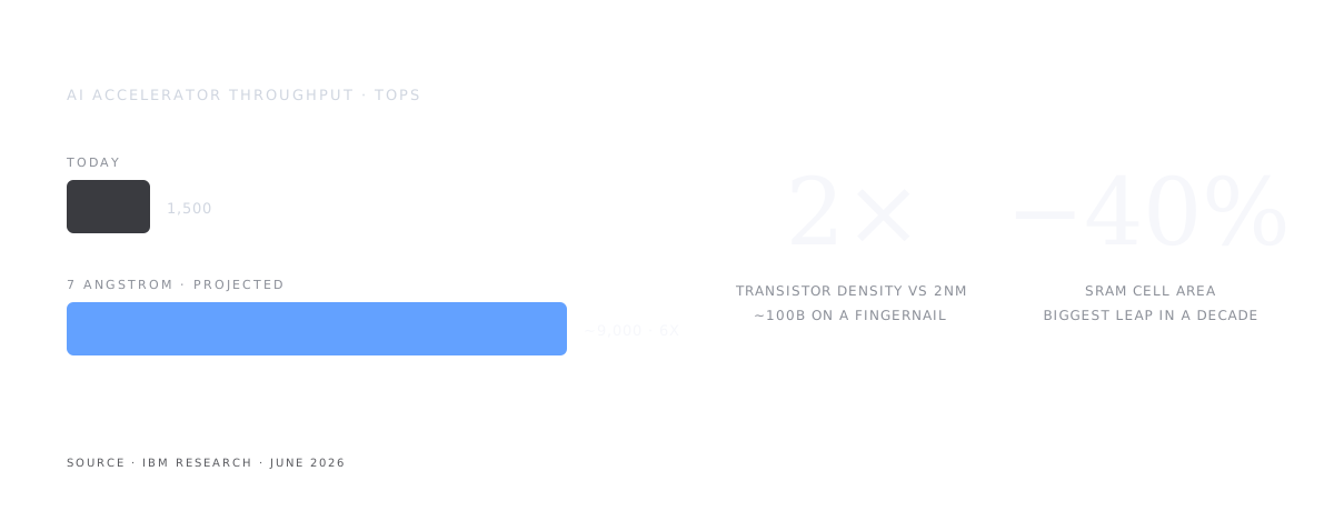
On June 25, IBM announced the world's first sub-1-nanometer chip technology: a 0.7nm (7 angstrom) node built on a new architecture it calls Nanostack. The headline number is nearly 100 billion transistors on a fingernail-sized die, roughly double the density of the 2nm chips IBM introduced in 2021.
What the paper actually shows
The interesting part is not the node label. Nanostack scales along the z-axis: instead of shrinking transistors further in two dimensions, it stacks them vertically in 3D, bonding layers with thin dielectric wafer bonding. Each layer can use a different channel material, so NFET and PFET devices are optimized independently instead of compromising on one.
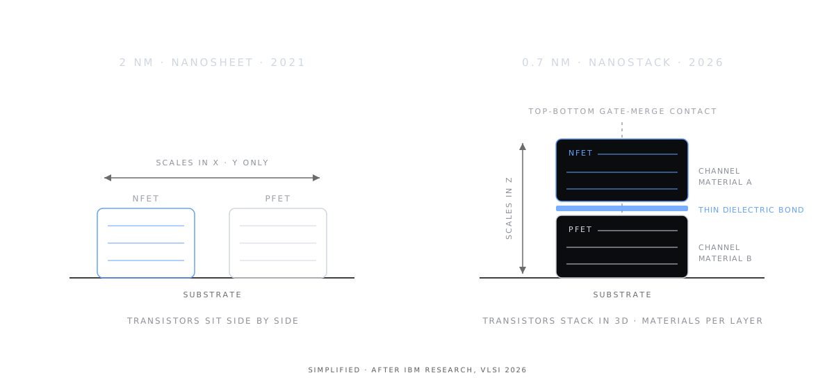
At VLSI 2026, IBM researchers presented working results, including staggered-channel Nanostack SRAM bitcells built around a top-bottom gate-merge contact fabricated on silicon for the first time, with about 40% SRAM scaling over current designs.
The numbers that matter
- Up to 50% more performance, or 70% better energy efficiency, than 2nm.
- AI accelerators on the node could reach roughly 9,000 TOPS, versus around 1,500 TOPS for today's parts.
- IBM estimates that kind of jump could cut frontier model training from about three months to a couple of weeks.
Commercial production is still an estimated five years out, and node names have long been marketing as much as measurement. But the direction is real.
Why we care
Crux is built on a simple bet: your most personal AI should be able to run on your hardware, right next to your data. The cloud is, and will stay, essential, it does remarkable things at a scale a single machine cannot. But you should not have to send your whole life to a data center just to get real capability. Every jump in transistor density and efficiency closes that gap, moving more of the same power onto the laptops and desktops people already own. A 9,000-TOPS accelerator in a consumer machine means AI on your own device can be as capable as the cloud, while your data never has to leave it. That is the future we are building for.